All published articles of this journal are available on ScienceDirect.

High Resolution Implantable Microsystem and Probe Design for Retinal Prosthesis
Abstract
By a retinal prosthesis, the researchers have been able to stimulate a limited number of neurons (around 100) by biphasic current stimulus to reproduce an image spatially by multiplexing technique. For functional restoration of sight (visual acuity 20/80), we are to stimulate at least 2500 neurons/mm2. We are far behind that target. The time required by biphasic current stimulus, the sequential stimulation by multiplexing technique, and the conventional probes used for stimulation limits our ability to stimulate large number of neurons and maintains the persistence of vision. To address this problem, we have designed high resolution donut probes and used them in designing neural implant chip (NIC) applying parallel multiplexing technique, which helped us stimulate large number of neurons. This paper presents the design of a donut probe and an implantable CMOS-based 5x5 array NIC to demonstrate that idea. This 5x5 array NIC is scalable to any larger array. It uses external clock, which makes it suitable for any data rate. The programmable biphasic width controller (BWC) used in this design is capable of generating various kinds of stimulus for stimulation. NIC doesn’t need address to route the pixels, which reduces the data transmission overhead. 0.5 µm CMOS technology is used to fabricate NIC with donut probes. Test results verify our technique of increasing the resolution.
1. INTRODUCTION
We know that photoreceptors of retina help us see. Due to age-related macular degeneration (AMD) or retinitis pigmentosa (RP), photoreceptors degenerate or cease to exist [1]. The goal of most of the researches is to develop a retinal prosthesis that will replace photoreceptors and pass visual signal to the next level. Epiretinal prosthesis pass signal to the ganglion cells, while subretinal prosthesis relay signals to the bipolar cells. Research is in progress on both kinds of prosthesis [2-16].
Biphasic current waveform (shown in Fig. (1)) is used to stimulate the neurons for its charge balancing capabilities. There are four parameters associated with this waveform. They are amplitude, width, interphase delay, and frequency. The typical values of all these parameters for retinal prosthesis as reported in various papers [1, 7, 17, 18] are: 10μA-600μA for amplitude, 100μs – 2ms for width, 0 –1ms for delay, and 10 –125Hz for frequency. Medical experiments have estimated that the equivalent impedance for the retinal tissue of RP and AMD patient is about 10Kohm [7]. The prosthesis, whether it is intended for epiretinal or subretinal implant, should be able to generate a biphasic current waveform of the above-mentioned parameters.
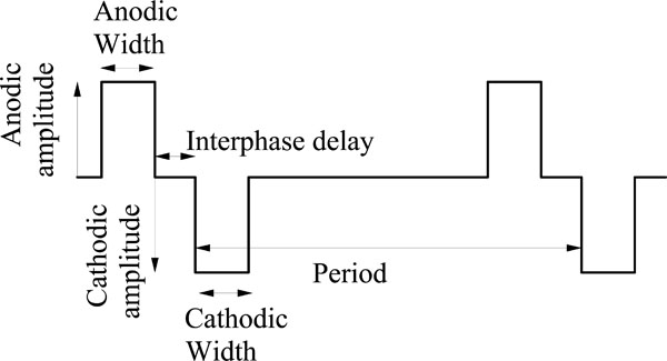
Biphasic current waveform
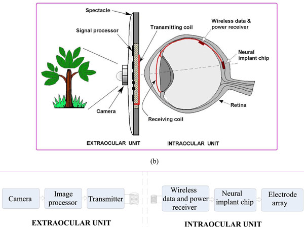
(a) Complete artificial vision restoration system (b) Block diagram of the retinal prosthesis
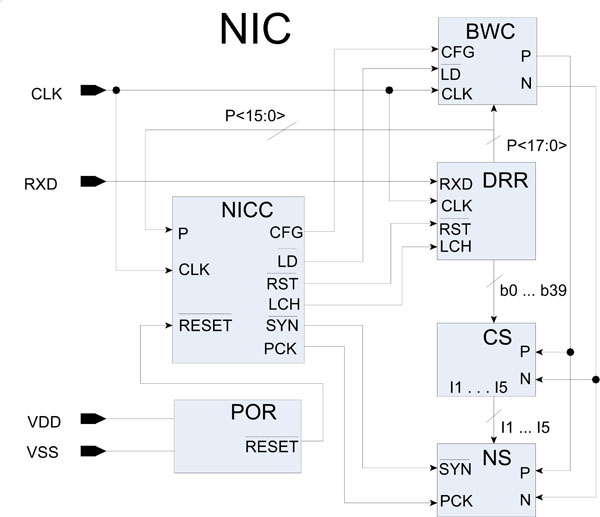
Block diagram of neural implant chip (NIC)
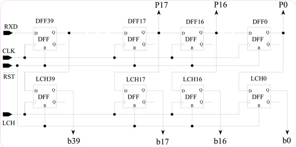
Schematic diagram of DRR
(a) Biphasic width controller (BWC), (b) Toggle flip flop (TFF)
(a) Current stimulator, (b) Regulated cascade current sink (RCCS)
Simulation and test of current stimulator
Structure of a donut probe
5x5 array neural stimulator (NS)
Block diagram of the NICC
(a) State diagram of the controller NICC (b) status of control signals at different states
Schematic diagram of power-on reset
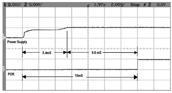
Test of POR. 5V was applied all of a sudden and monitors the reset. Trace 1 is the transient voltage rise and Trace 2 is the reset
Microscopic view of the test module of 5x5 array NIC
Test setup of NIC. Microcontroller (PIC) is programmed with the data of letter “L” as shown in the table on left of the figure. PIC sends this data to the NIC continuously to stimulate the neurons
Biphasic pulse width control test. Widths generated by configuration word (a) 0x033DF3 (b) 0x033DFB (c) 0x03BEFF (d) 0x03FEFB (e) 0x03BFFB

Variable data loaded (a) P21 = 0x20, P22 = 0x80 (b) P52 = 0x20, P53 = 0x80. Measured amplitudes are 0.8V and 3.2V respectively
Data loaded is 0x40 in each channel. Measured amplitude is 1.6V
We see some successes of retinal stimulation by only limited number of electrodes [7, 19, 20]. So far the vision is limited to creation of stars like phosphene by an array of 5x5 [7] or 10x10 [19]. In terms of density, it is only 20 electrodes/mm2 [19]. For functional restoration of sight, the required visual acuity is 20/80, which is equivalent to 2500 pixel/mm2 [21]. That means we are to excite as many as 2500 electrodes/mm2. We are far behind that target. Two main factors that are limiting our ability to achieve high resolution are the conventional electrodes that we are using for stimulation and sequential stimulation by biphasic stimulus.
Electrodes are the interface between microsystems and bio-cells. The ideal interface is one-to-one interface. Though we have been able to establish some sort of interface after so many years of research, it is very crude. Neurons are millions in numbers, whereas our successfully built prostheses have only a few hundred electrodes at best. Though we have micro- and nano-technologies, we couldn’t build prosthesis with effective resolution. Effort is being made to increase the resolution. The resolution depends on a number of factors—like the geometry of the probes, the type of prosthesis, extends of damage of the patient, the distance of the probes from the target cells, the amplitude/duration/frequency of stimulus, etc. All these play a role in controlling the resolution. But what we have found is that the geometry of the probe plays a major role [22]. Conventional probes [7, 17, 20, 23] mostly used to stimulate neurons are pointing, monopolar, bipolar, etc. We have found that the resolutions of these probes are not good. The electric field generated by these probes spread wider reducing the resolution. We have designed a donut probe, which is far better than the conventional probes [22, 24]. In our study, we have found that donut probe has 33% better resolution and 44% lesser potential drop (lesser resistance) than the conventional probes [22, 24]. In section 7, the design of such a probe is given. Another thing that we want in our probe is the lowest possible stimulation current to generate action potential. The thresholds found by various research groups to generate action potential vary widely. It varies from 0.15μA to 1121μA, and the related pulse duration varies from 75μs to 2ms [8, 17]. The reasons of these wide variations most probably are the condition of the individual subjects, the type of prosthesis (epi-retinal or sub-retinal) they used, the type of probes (pointing, monopolar, bipolar, etc.), the geometry of the probe, and the location of the probe with respect to the target cells. If the geometry of the probe is bigger than what is required then the threshold current would increase or if the probe is smaller, then the threshold current could decrease, but may create unsafe current density in the electrode and tissue interface. The spacing between stimulating and return electrodes also affects the threshold. In designing probe, all these must be taken into consideration. In [22], a methodology of designing a donut probe and an array of probes is developed, which has been utilized to optimize all the parameters.
The time required by biphasic stimulus, and sequential stimulation by multiplexing technique also limits our ability to stimulate a large number of neurons, and maintain the persistence of vision. Typical values of biphasic stimulus suggest that the duration of biphasic pulse could be as long as 5ms. The persistence of vision (1/30th of a second) gives us 33.33ms to complete one frame. If we apply multiplexing technique, and stimulate each neuron for 5ms, then only 6 electrodes could be stimulated within this time frame. So large scale stimulation required by a retinal prosthesis is a big challenge. Simple multiplexing technique won’t work for large scale stimulation. To address this problem, parallel multiplexing technique is applied [1] is also trying the similar approach. By this technique it is possible to excite a large number of neurons within the persistence of vision. Though 6 electrodes could be excited through sequential multiplexing technique, in this design only 5 electrodes are considered to allow extra time for synchronization, which will be explained later. So the total number of electrodes is divided into 5 groups, and parallel stimulation is applied to all the electrodes of a group, and multiplexing among the groups. In this way, it is possible to excite as many neurons as we want by biphasic current stimulus, and still maintain the persistence of vision. To demonstrate this idea, a 5x5 array NIC is designed, fabricated, and tested. It needs only 4 wires to interface with the wireless receiver, a huge reduction of number of wires compare to flexible retinal implant [25]. It is scalable to a larger array. It uses external clock for its timing making it suitable for any data rate. It has a programmable biphasic width controller (BWC), which can generate monophasic or biphasic current stimulus with or without interphase delay.
2. SYSTEM OVERVIEW
The overall system of a retinal prosthesis and its block diagram are shown in Fig. (2). It is basically a two units systems – one is extraocular and another intraocular unit—magnetically coupled together. The intraocular unit is implanted inside the eye, while the extraocular unit is mounted on the eyeglasses. Extraocular unit has a CCD camera, an image processor, an encoder, and a transmitter built on the eyeglass. High-resolution image from a CCD camera is reduced to lower resolution matching the array of electrodes by image processor, which is then encoded and transmitted wirelessly after time multiplexing. The intraocular unit is implemented in two chips—one is wireless receiver and another NIC as shown in Fig. (2). Wireless receiver recovers each pixel and clock, and generates necessary power for the chip from its 13.56MHz carrier frequency. NIC is implanted in the retina to stimulate the healthy cells. It converts each pixel into biphasic current stimulus, and applies it to a 5x5 array arranged in 2D to reproduce a form vision.
3. DESIGN OF PROSTHESIS
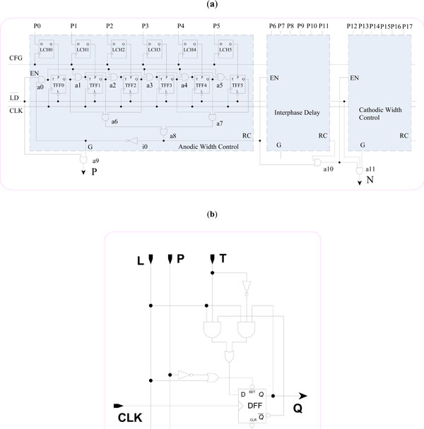
The block diagram of the NIC is shown in Fig. (3). Four main functional blocks of the chip are data receiving register (DRR), biphasic width controller (BWC), current stimulator (CS), and neural stimulator (NS). These blocks are controlled by the neural implant chip controller (NICC). In the following sections, the detailed design and function of each block are presented.
3.1. Data Receiving Register (DRR)
DRR is designed (Fig. 4) to handle 40 bits of data. 5x5 array NS has 5 rows and 5 columns. If each pixel is 8 bits deep, then the required total length of a row of DRR is 40 bits. DRR is a double buffering first-in first-out (FIFO) serial to parallel converter. The 40-bit data is serially inputted to the 40-bit shift register (DFF), then latch to the 40-bit latch register (LCH).
3.2. Biphasic Width Controller (BWC)
The design of BWC is shown in Fig. (5). It is designed with three similar units for controlling anodic width (P), interface delay, and cathodic width (N). Each unit has a memory register (LCH0-LCH5) and a synchronous binary counter composed of 6 toggle flip-flops (TFF0-TFF5) as shown in Fig. (5). When input L of TFF is low, bit P is loaded in DFF, else it toggles with CLK when T is high. EN is the count enable, and RC is the ripple carry of the counter. The input CFG is used to latch the configuration bits (P0-P17) in the memory register, while input to load the configuration bits in the counter.
When is pulled low briefly, the counters are loaded with configuration bits from memory registers, and anodic width counter starts counting from its loaded number with the rising edge of CLK. On reaching count 63, the output RC goes high enabling interface delay counter, setting P low, and locking anodic width counter by i0. Similarly, interphase delay counter enables cathodic width counter when it counts 63, and sets N high allowing generation of cathodic width, as RC of interphase delay counter is high at this time. Cathodic width counter starts counting from its loaded number with the rising edge of CLK and on count 63, it sets N low locking itself by feed back inverter. At the end, all the three counters get locked and remain so till they receive another reset by , which is initiated at the beginning of next row. As counters stop at 63 from the programmed bits, the unit should be programmed with lower number for longer width or delay, as the width or delay is the difference between the set number and 63. With this design, we can generate only anodic or cathodic pulse by setting the other to zero or biphasic pulse without delay by setting interphase delay to zero. The width can be given by:
Andonic/cathodic/interphase delay in time
where, f is the clock frequency.
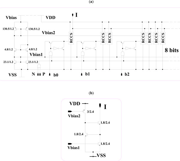
3.3. Current Stimulator (CS)
The design of CS is shown in Fig. (6). It is an 8-bit current converter and converts binary-weighted data (b0…b7) into equivalent analog current (I). It is designed using regulated cascode current sink (RCCS) as shown in Fig. (6), which uses negative feedback to stabilize the output current, and to increase the output impedance. Control of Vbias1 by input could be enough, but the additional control by the OR gate helped us reduce the current surge during switching. CS is design for a resolution of 2.5µA; for 10KΩ load, it can deliver 640µA at 7V, or 484µA at 5V for full 8-bit data.
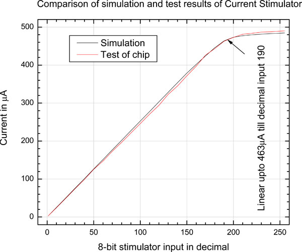
The simulation and test of CS is plotted in Fig. (7). The test result is very close to the simulation result. CS is tested with 5V and 10KΩ load for the whole range of 8-bit data. The test results reveal that the CS has 2.5µA resolution, and is linear up to 463 µA corresponding to decimal input of 190. Maximum current is 489 µA at decimal input value of 255.
3.4. Neural Stimulator (NS)
Probe Design:
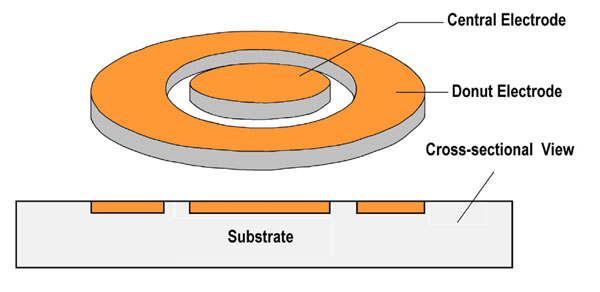
The structure of donut probe is shown in Fig. (8). It has two flat electrodes—one is central and another donut electrode. Both these electrodes are embedded in the silicon substrate with the top surface exposed to the tissue. So these electrodes conduct current through the top surface only. The surface areas of both the electrodes are made equal to let them have equal current carrying capacity.
The specifications of the donut probe design are given in Table 1. Details are given in [22].
Specifications of Donut Probe and Probe Array for 20µm Penetration
| Parameters/Dimensions | Value |
| Penetration | 20µm |
| Stimulating current | 15.8µA |
| Radius of central electrode (r) | 15µm |
| Spacing bet. central & donut electrodes | 20µm |
| Inner radius of donut electrode (r1) | 35µm |
| Outer radius of donut electrode (r2) | 38µm |
| Thickness of electrodes | 2µm |
| Mini. spacing between two probes | 150µm |
| Resolution | 150µm×150µm |
| Material | IrOx |
Protocol of Data Transmission
| Start Word | xxxx xxxx | xxxx xxxx | xxxx xxxx | 1110 1110 | 1110 1110 |
| Config. Word | xxxx xxxx | xxxx xxxx | xxxx xxpp | pppp i i i i | i i nn nnnn |
| Row 1 Data | dddd dddd | dddd dddd | dddd dddd | dddd dddd | dddd dddd |
| : | |||||
| Row 5 Data | dddd dddd | dddd dddd | dddd dddd | dddd dddd | dddd dddd |
| Sync Word | xxxx xxxx | xxxx xxxx | xxxx xxxx | 1010 1010 | 1010 1010 |
NICµs Specifications and Performance for 13.889 KHz Clock
| Parameters | Specification/Performance |
| Technology | CMOS 0.5 mm |
| Die size | 3 mm x 3 mm |
| Probe type | Donut probe |
| Number of probes | 5 x 5array (25 probes) |
| Resolution of probes | 150 µm x 150 µm |
| Total area of probes | 750 µm x 750 µm |
| Number of current stimulator | 5 |
| Current Stimulator | 8 bits |
| Supply voltage | 5V (or 3V) |
| Resolution of current stimulator | 2.5 µA |
| Current stimulator output (for input 0-BE) | 0-400 µA†(Linear range) |
| Current stimulator output (for max. input FF) | 430 µA†(max.) |
| Type of waveform (software configurable) | Monophasic (anodic) |
| Monophasic (cathodic) | |
| Biphasic (with interphase delay) | |
| Biphasic (without interphase delay) | |
| Pulse width (programmable by 6-bit counter) | 0-2.88 ms‡ |
| Data rate | 13.889 Kbits/sec‡ |
| Frame rate | 55.94 frames/sec‡ |
| Power consumption (no load) | 1.59 mW at 3V |
| 13.70 mW at 5V | |
| Power consumption (full load) | 2.44 mW at 3V |
| 18.65 mW at 5V |
†For 5V supply.
‡For clock frequency 13.889 KHz
It has been shown in [22, 24] that donut probe has better electric field penetration, lesser spreading of electric field (means higher resolution), and posses least resistance to the current flow compare to the traditional electrodes. Donut probe has 33% better resolution, 44% lesser resistance than many of the conventional probes. In our neural stimulator circuit design, we have used this probe to improve the resolution.
Circuit Design:
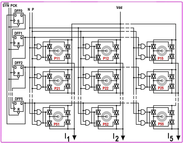
The design of 5x5 array NS is shown in Fig. (9). It has an array of probes (P11-P55), and a decoder (DFF1-DFF5). Each probe has four switches, which are controlled by two AND gates, which are controlled by the decoder and the BWC. Probe mentioned in Fig. (8) is grown based on CMOS technology. The central and donut electrodes are fabricated on top metal-3 layer. Beneath the electrodes, the switches and gates are grown. There are five current stimulating buses (I1 to I5); each of them carries the time-multiplexed stimulus for all the probes of a column. PCK is the clock for the decoder, which is 40 times slower than the data clock CLK. With start ( low), decoder points to DFF0 as it is a set DFF, while other are clear DFFs. In the next PCK cycle (which occurs after 40 CLK cycles, during which data of first row are loaded and latched in DRR, and converted into analog currents (I1–I5) by CS), decoder points to the first row (output of DFF1 is high) and five different stimulus currents are applied to the five probes of the first row, the duration of which are controlled by P and N. Before the rising edge of next PCK cycle, DRR is again loaded with new data for the next row selected by the decoder (DFF2), which are then converted into analog currents (I1–I5) by CS, and are applied to the probes of new row. This pattern goes on till the end of 5th row, and then it starts all over again. So this way, parallel stimulation is being applied to all the probes of a row, and multiplexing among the rows.
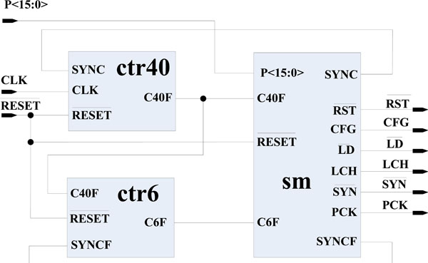
3.5. Neural Implant Chip Controller (NICC)
NICC is the main controller of the NIC. It controls BWC, DRR, CS, and NS through outputs , CFG, , LCH, , and PCK. It has three inputs ( , CLK, and P<15: 0>). It monitors part of the received data in the DRR through P<15: 0>. The block diagram of NICC is shown in Fig. (10). It is composed of two counters (ctr40 and ctr6), and one state machine (sm). ctr40 keeps track of the 40 bits data of a row. When 40 bits are shifted in the DRR, it issues a pulse (C40F) for half cycle. This pulse works as a clock for sm and ctr6. ctr6 keeps count of rows. When it counts 6 (5 rows and 1 sync packets), it generates a pulse (C6F) for half a cycle, signaling sm of completing a frame. Output clears the shift register and latch of DRR, CFG configures the BWC, loads the synchronous counter of BWC at the beginning of stimulation of each row, LCH latches 40 bits of data of a row in DRR, and synchronizes the scanning process of NS. PCK works as a clock for NS. Output SYNC is used to reset the ctr40 at the end of count; while output SYNCF reset ctr6 when synchronization word is received at the end of 5th row.
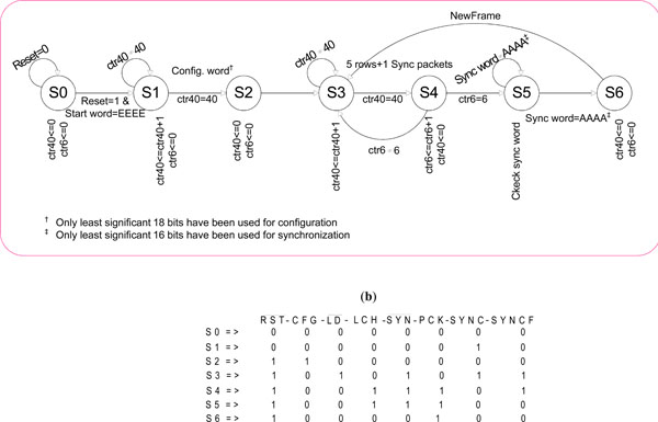
The state machine sm can be explained with state diagram and status of control signals shown in Fig. (11). When is pulled low briefly, sm is forced to state S0 or if it is in any other state it returns to S0. In this state, all the control outputs are zero. The sm monitors P<15: 0> and stays at S0 till it finds the start word 0xEEEE. As soon as it senses the start word, it moves to S1 enabling the counter ctr40 by pulling SYNC high. When ctr40 counts 40, the sm moves to S2, where is released and least significant 18 bits are latched by CFG as configuration word in BWC. sm then moves to S3 at the rising edge of clock CLK. and are pulled high in this state enabling the synchronous counter in BWC and releasing the scanning mechanism of NS respectively. Data of the first row starts shifting in DRR. When 40 bits are counted, sm moves to S4 and LCH latches these data in DRR, and PCK advances the NS decoder to point to the first row. C40F increases the count of ctr6 by one and check whether C6F flag is true. If the C6F flag is false, the sm slides back to S3 and starts counting the data of second row. Thus the sm moves back and forth till the data of all the 5 rows and the sync word are received; sm then moves to S5. Data which is in DRR at this stage is the synchronization word. This word is checked with the preset word 0xAAAA. When sm finds the matching word, it advances to S6 resetting ctr40 and ctr6. sm then moves back to S3 in the rising edge of next clock (CLK), and starts a new frame.
The data transmission protocol of NIC is given in Table 2. ‘x’ stands for the padding bits, ‘d’ for the data of the rows, ‘p’, ‘i’, and ‘n’ stand for anodic, interface delay and cathodic width bits respectively. The data transmission starts with start word, which is set here as ‘1110 1110 1110 1110’2 (0xEEEE), followed by the configuration, data, and ends with the sync packet, which is “1010 1010 1010 1010”2 (0xAAAA). Least significant 8 bits are the data of the 5th probe, followed by the data of 4th, 3rd, 2nd, and 1st probe. In the next frame, the start and configuration words are not sent; transmission start directly with the data of row 1, row 2, …, and row 5, and ends with sync word.
3.6. Power on Reset (POR)
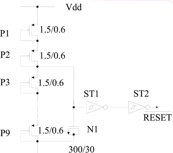
To save silicon space, POR is designed with nine diode-connected transistors instead of traditional resistors, a MOS capacitor instead of ceramic capacitor, and two Schmitt triggers as shown in Fig. (12)[26] has designed POR with diode string but used comparator. Instead of applying the total voltage, a part of it [input voltage = (7/9)×Vdd = (7/9)×5V = 3.88V] is applied to reduce the size of MOS capacitor added to the input of the Schmitt trigger to delay the rise of supply voltage. Usually 3-4ms delay [26] is what we need to ensure the recovery of supply voltage and ensure a reset during this period.
POR is tested by applying 5V dc suddenly and monitoring the transient rise of the power and the reset. The result is presented in Fig. (13). From the plots, we see that the voltage rose to its applied value within 5.4 ms after switching, while reset stayed active for further 9.6ms after reaching 5V. Though outside voltage rose to 5V within 5.4ms, the MOS capacitor delayed reaching threshold for another 9.6ms. This longer delay will ensure better reset of the system under rated power supply.
3.7. Neural Implant Chip (NIC)
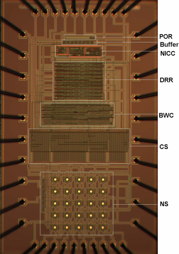
The microscopic view of NIC is shown in Fig. (14). It is designed according to the Fig. (3). To drive heavy loads, buffers are added. To test NIC, a test module is designed with many test points wired out of the chip. 0.5μm CMOS technology is used to design it in an area of 1.5mmX 3mm.
4. Test of neural implant chip (NIC)
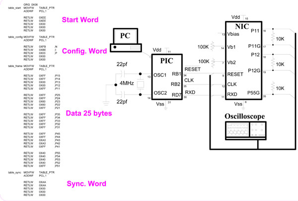
The test setup of NIC is shown in Fig. (15). The setup shows only the connections of a personal computer (PC operating on Windows XP), a microcontroller (PIC16F877 from Microchip Inc.), NIC (chip under test), and the oscilloscope (54622D from Agilent Technologies). To program the microcontroller, an evaluation board from Matrix Multimedia, UK, is used. Also to read the current flow through the loads (10Kohm resistors shown at the output of NIC), instrument amplifiers (not shown in the figure) are used. The PIC and NIC both are powered by 5V dc i.e. Vdd = 5V and Vss = 0V. The instrument amplifier is powered by Vdd = 10V, Vss = 0, and Vref = 5V. 10V is used in instrument amplifier to have a swing of 5V in both the directions from mid-point, giving us the ability to read full drop of voltage across 10Kohm generated by anodic or cathodic waveform. Data table of Fig. (15) represent an image of letter ‘L’. To reproduce it, we are to transmit this table to the NIC. Instead of transmitting data from this table, a real time data can be read from a port of PIC (connected to a DSP) and send it directly. In this test, NIC is tuned to 2.5μA resolution corresponding to each binary digit. A clock of frequency 7.353 KHz is used.
Basically 3 main tests are carried out in addition to checking the reset, start word, and synchronization word. They are:
Biphasic pulse width control test:
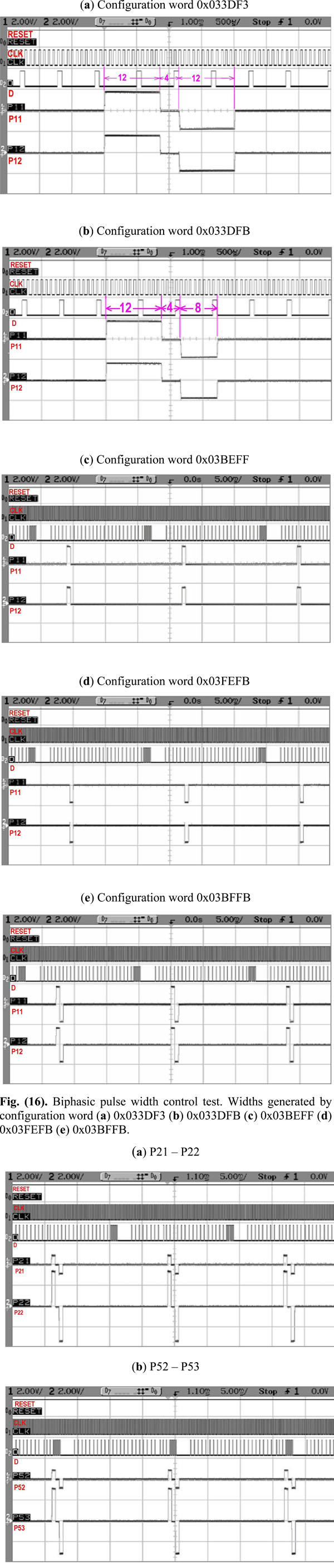
This test is carried out by programming different configuration words. The widths set by configuration word 0x033DF3 are shown in Fig. (16) and that set by 0x033DFB are shown in Fig. (16). The configuration word 0x033DF3 will set anodic and cathodic widths each to 12 cycles, and interphase delay to 4 cycles. From Fig. (16), we also see that they are 12 cycles long. Similarly configuration word 0x033DFB will set anodic width 12, cathodic width 8, and the interphase delay to 4 cycles and this is what we have in the Fig. (16). In Fig. (16,d) monophasic waveforms are generated by the configuration words 0x03BEFF and 0x03FEFB respectively. The configuration word 0x03BFFB has created biphasic waveform without delay as shown in Fig. (16), because it sets the interphase delay to zero.
Biphasic pulse amplitude control test:
The data of each probe (P11, P12...P55) mentioned in Fig. (15) sets the amplitude of the biphasic waveform. By setting different values for these data, different amplitudes are tested. We have tested for data 0x00, 0x01, 0x02, 0x04, 0x08, 0x10, 0x20, 0x40, 0x80, and 0xFF for each row. In Fig. (17), the outputs for data 0x20 and 0x80 in two different probes are presented. Measured output amplitudes are 0.4V and 3.2V respectively. This voltage across 10Kohm represents a current of (0.4V/10KOhm) 40μA and 320μA which is 16 and 128 times stronger than the 2.5μA respectively. This result shows the linear dependence of the data with the amplitude. From other tests, it is found that the amplitude of the pulse is proportional to the data from 0x01 to 0xB0; the data above 0xB0 shows different degree of amplitude saturation of different channels as predicted from the test of CS mentioned in section 3.3. So for linear response, we are to avoid setting data above 0xB0. For maximum value of data i.e. 0xFF, the maximum amplitude recorded is 4.3V. This is equal to 430μA, which is close to the test result obtained in section 3.3.
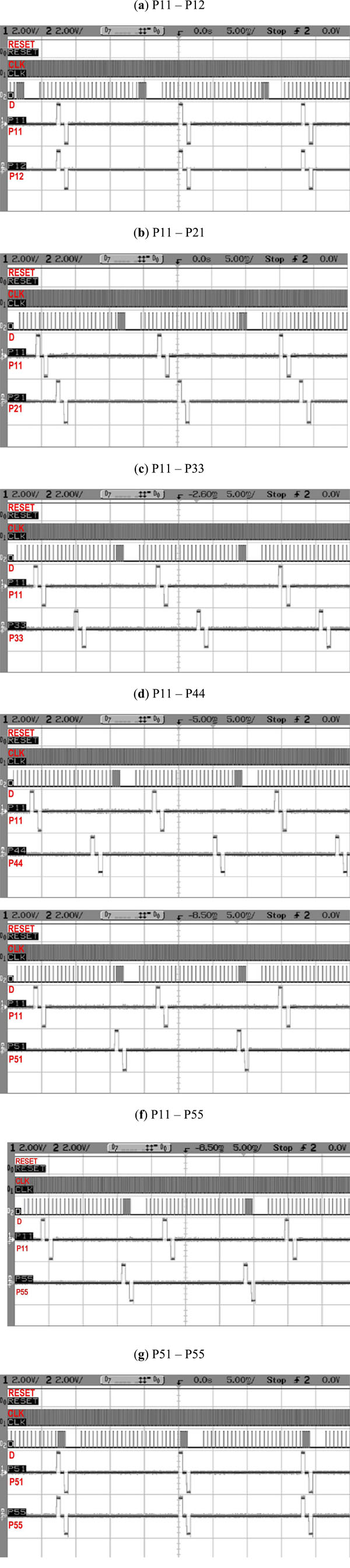
Parallel multiplexing stimulation test:
Tests of parallel multiplexing stimulation are also presented in Fig. (18). In this test, it is found that all the probes of the same row (e.g. P11 and P12 of row1 or P51 and P55 of row 5 as shown in 18(a) and (g)) got activated simultaneously, while probes of different rows (e.g. P11 and P21, or P11 and P33, or others as shown in Fig. (18)) took turn. It means the probes of a row are showing parallel stimulation while probes of different rows exhibiting multiplexed stimulation. The time difference between two consecutive rows (e.g. row 1 and row 2 as shown in Fig. (18)) is 40 cycles, while time difference between row 1 and row 5 (e.g. P11 from row1 and P55 from row5 as shown in Fig. (18)) is 5 times than the consecutive rows. This verifies that the parallel multiplexing stimulation is working.
The specifications and performance of NIC are given in Table 3 for 13.889 KHz clock used for testing.
5. CONCLUSION
A prototype 5x5 array neural implant chip is designed, fabricated, and tested. 0.5μm CMOS technology is used to fabricate it. The chip is fabricated through MOSIS. The vital part of chip i.e. neural stimulator is scaleable i.e. to increase the array size we are to add as many columns of probes as we want and stimulate them with the others by biphasic current stimulus simultaneously maintaining the persistence of vision. The parallel multiplexing technique thus make us possible to increase the 5×5 array, but does not allow us to increase the row as that will exceed the limit of persistence of vision. It is to note here that with the addition of each column, one additional CS is required with the bigger DRR. Now, with this solution of microsystem, the limitation lies with the probes. Donut probes, which have better resolution than the conventional probes, are used in this design. These probes definitely helped us crowd more probes in a smaller area; but to increase the resolution further, we are to place the probes as close to the target cells as possible so that the required electric field penetration (here 20μm) is reduced, which will reduce the required stimulation current (here 15.8μA) and help us increase the probe resolution (which is 150μm×150μm for 20μm penetration) further.
Unlike others, our NS has onboard donut probes that eliminate the need of wiring them from the chip. It is also possible to design the microsystems of wireless receiver in NIC to make it completely wireless or connect NIC to the wireless receiver through only four wires (CLK, RXD, Vdd, and Vss,). NIC uses external clock making it suitable to tune it to any data rate. For stimulation, NIC doesn’t need address as is found in most of the prostheses design. Sequential stimulation of each row by the clock is saving us from the wireless address transmission overhead. Programmable BWC and high resolution CS has made us possible to fine tune NIC to suit the need of wide varieties of patients